Saturday, 19 March 2011 20:40

General Profile

Rate this item
(0 votes)

The diversity of processes and products within the microelectronics and semiconductor industry is immense. The focus of the occupational health and safety discussion in this chapter centres on semiconductor integrated circuit (IC) production (both in silicon-based products and valence III-V compounds), printed wiring board (PWB) production, printed circuit board (PCB) assembly and computer assembly.

The industry is composed of numerous major segments. The Electronics Industry Association uses the following delineation in reporting data on pertinent trends, sales and employment within the industry:

  • electronic components
  • consumer electronics
  • telecommunications
  • defence communications
  • computers and peripheral equipment
  • industrial electronics
  • medical electronics.


Electronic components include electron tubes (e.g., receiving, special-purpose and television tubes), solid-state products (e.g., transistors, diodes, ICs, light-emitting diodes (LEDs) and liquid-crystal displays (LCDs)) and passive and other components (e.g., capacitors, resistors, coils, transformers and switches).

Consumer electronics include television sets and other home and portable audio and video products, as well as information equipment such as personal computers, facsimile transmission machines and telephone answering devices. Electronic gaming hardware and software, home security systems, blank audio and video cassettes and floppy disks, electronic accessories and total primary batteries also fall under the consumer electronics heading.

In addition to general purpose and specialized computers, computers and peripheral equipment includes auxiliary storage equipment, input/output equipment (e.g., keyboards, mice, optical scanning devices and printers), terminals and so on. While telecommunications, defence communications and industrial and medical electronics utilize some of the same technology these segments also involve specialized equipment.

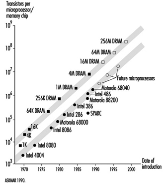
The emergence of the microelectronics industry has had a profound impact on the evolution and structure of the world’s economy. The pace of change within industrialized nations of the world has been greatly influenced by advances within this industry, specifically in the evolution of the integrated circuit. This pace of change is graphically represented in the timeline of the number of transistors per integrated circuit chip (see figure 1).

Figure 1. Transistors per integrated circuit chip

MICO10F1

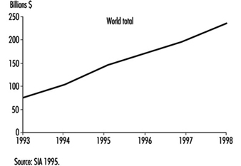
The economic importance of worldwide semiconductor sales is significant. Figure 2 is a projection by the Semiconductor Industry Association for worldwide and regional semiconductor sales for 1993 to 1998.

Figure 2. Worldwide semiconductor sales forecast

MICO10F2

The semiconductor IC and computer/electronics assembly industries are unique compared to most other industrial categories in the relative composition of their production workforces. The semiconductor fabrication area has a high percentage of female operators that run the process equipment. The operator-related tasks typically do not require heavy lifting or excess physical strength. Also, many of the job tasks involve fine motor skills and attention to detail. Male workers predominate in the maintenance-related tasks, engineering functions and management. A similar composition is found in the computer/electronics assembly portion of this industry segment. Another unusual feature of this industry is the concentration of manufacturing in the Asia/Pacific area of the world. This is especially true in the final assembly or back-end processes in the semiconductor industry. This processing involves the positioning and placement of the fabricated integrated circuit chip (technically known as a die) on a chip carrier and lead frame. This processing requires precise positioning of the chip, typically through a microscope, and very fine motor skills. Again, female workers predominate this part of the process, with the majority of worldwide production being concentrated in the Pacific Rim, with high concentrations in Taiwan, Malaysia, Thailand, Indonesia and the Philippines, and growing numbers in China and Vietnam.

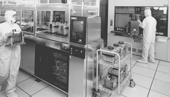
The semiconductor IC fabrication areas have various unusual properties and characteristics unique to this industry. Namely, the IC processing involves extremely tight particulate control regimens and requirements. A typical modern IC fabrication area may be rated as a Class 1 or less cleanroom. As a method of comparison, an outdoor environment would be greater than Class 500,000; a typical room in a house approximately Class 100,000; and a semiconductor back-end assembly area approximately Class 10,000. To attain this level of particulate control involves actually putting the fabrication worker in totally enclosed bunny suits that have air supply and filtration systems to control the levels of particulates generated by the workers in the fabrication area. The human occupants of the fabrication areas are considered very potent generators of fine particulates from their exhaled air, shedding of skin and hair, and from their clothing and shoes. This requirement for wearing confining clothing and isolating work routines has contributed to employees feeling like they are working in a “non-hospitable” work environment. See figure 3. Also, in the photolithographic area, the processing involves exposing the wafer to a photoactive solution, and then patterning an image on the wafer surface using ultraviolet light. To alleviate unwanted ultraviolet (UV) light from this processing area, special yellow lights are used (they lack the UV wavelength component normally found in indoor lighting). These yellow lights help to make the workers feel they are in a different work environment and can possibly have a disorienting affect on some individuals.

Figure 3. A state-of-the-art cleanroom

MIC010F3


Back

Read 3871 times Last modified on Saturday, 30 July 2022 23:54

" DISCLAIMER: The ILO does not take responsibility for content presented on this web portal that is presented in any language other than English, which is the language used for the initial production and peer-review of original content. Certain statistics have not been updated since the production of the 4th edition of the Encyclopaedia (1998)."

Contents

Microelectronics and Semiconductors References

American Conference of Governmental Industrial Hygienists (ACGIH). 1989. Hazard Assessment and Control Technology in Semiconductor Manufacturing. Chelsea, MI: Lewis Publishers.

—. 1993. Hazard Assessment and Control Technology in Semiconductor Manufacturing II. Cincinnati, OH: ACGIH.

—. 1994. Documentation of Threshold Limit Value, Rosin Core Solder Thermal Decomposition Products, as Resin Acids-Colophony. Cincinnati, OH: ACGIH.

American National Standards Institute (ANSI). 1986. Safety Standard for Industrial Robots and Industrial Robot Systems. ANSI/RIA R15.06-1986. New York: ANSI.

ASKMAR. 1990. Computer Industry: Critical Trends for the 1990’s. Saratoga, CA: Electronic Trend Publications.

Asom, MT, J Mosovsky, RE Leibenguth, JL Zilko, and G Cadet. 1991. Transient arsine generation during opening of solid source MBE chambers. J Cryst Growth 112(2-3):597–599.

Association of the Electronics, Telecommunications and Business Equipment Industries (EEA). 1991. Guidelines on the Use of Colophony (Rosin) Solder Fluxes in the Electronics Industry. London: Leichester House EEA.

Baldwin, DG. 1985. Chemical exposure from carbon tetrachloride plasma aluminum etchers. Extended Abstracts, Electrochem Soc 85(2):449–450.

Baldwin, DG and JH Stewart. 1989. Chemical and radiation hazards in semiconductor manufacturing. Solid State Technology 32(8):131–135.

Baldwin, DG and ME Williams. 1996. Industrial hygiene. In Semiconductor Safety Handbook, edited by JD Bolmen. Park Ridge, NJ: Noyes.

Baldwin, DG, BW King, and LP Scarpace. 1988. Ion implanters: Chemical and radiation safety. Solid State Technology 31(1):99–105.

Baldwin, DG, JR Rubin, and MR Horowitz. 1993. Industrial hygiene exposures in semiconductor manufacturing. SSA Journal 7(1):19–21.

Bauer, S, I Wolff, N Werner, and P Hoffman. 1992a. Health hazards in the semiconductor industry, a review. Pol J Occup Med 5(4):299–314.

Bauer, S, N Werner, I Wolff, B Damme, B Oemus, and P Hoffman. 1992b. Toxicological investigations in the semiconductor industry: II. Studies on the subacute inhalation toxicity and genotoxicity of gaseous waste products from the aluminum plasma etching process. Toxicol Ind Health 8(6):431–444.

Bliss Industries. 1996. Solder Dross Particulate Capture System Literature. Fremont, CA: Bliss Industries.

Bureau of Labor Statistics (BLS). 1993. Annual Survey of Occupational Injuries and Illnesses. Washington, DC: BLS, US Department of Labor.

—. 1995. Employment and Wages Annual Averages, 1994. Bulletin. 2467. Washington, DC: BLS, US Department of Labor.

Clark, RH. 1985. Handbook of Printed Circuit Manufacturing. New York: Van Nostrand Reinhold Company.

Cohen, R. 1986. Radiofrequency and microwave radiation in microelectronics industry. In State of the Art Reviews—Occupational Medicine: The Microelectronics Industry, edited by J LaDou. Philadelphia, PA: Hanley & Belfus, Inc.

Coombs, CF. 1988. Printed Circuits Handbook, 3rd ed. New York: McGraw-Hill Book Company.

Content, RM. 1989. Control methods for metal and metalloids in III-V materials vapor-phase epitaxy. In Hazard Assessment and Control Technology in Semiconductor Manufacturing, edited by the American Conference of Governmental Industrial Hygienists. Chelsea, MI: Lewis Publishers.

Correa A, RH Gray, R Cohen, N Rothman, F Shah, H Seacat, and M Corn. 1996. Ethylene glycol ethers and risks of spontaneous abortion and subfertility. Am J Epidemiol 143(7):707–717.

Crawford, WW, D Green, WR Knolle, HM Marcos, JA Mosovsky, RC Petersen, PA Testagrossa, and GH Zeman. 1993. Magnetic field exposure in semiconductor cleanrooms. In Hazard Assessment and Control Technology in Semiconductor Manufacturing II. Cincinnati, OH: ACGIH.

Escher, G, J Weathers, and B Labonville. 1993. Safety design considerations in deep-UV excimer laser photolithography. In Hazard Assessment and Control Technology in Semiconductor Manufacturing II. Cincinnati, OH: American Conference of Governmental Industrial Hygienists.

Eskenazi B, EB Gold, B Lasley, SJ Samuels, SK Hammond, S Wright, MO Razor, CJ Hines, and MB Schenker. 1995. Prospective monitoring of early fetal loss and clinical spontaneous abortion among female semiconductor workers. Am J Indust Med 28(6):833–846.

Flipp, N, H Hunsaker, and P Herring. 1992. Investigation of hydride emissions during the maintenance of ion implantation equipment. Presented at the June 1992 American Industrial Hygiene Conference, Boston—Paper 379 (unpublished).

Goh, CL and SK Ng. 1987. Airborne contact dermatitis to colophony in soldering flux. Contact Dermatitis 17(2):89–93.

Hammond SK, CJ Hines MF Hallock, SR Woskie, S Abdollahzadeh, CR Iden, E Anson, F Ramsey, and MB Schenker. 1995. Tiered exposure assessment strategy in the Semiconductor Health Study. Am J Indust Med 28(6):661–680.

Harrison, RJ. 1986. Gallium arsenide. In State of the Art Reviews—Occupational Medicine: The Microelectronics Industry, edited by J LaDou Philadelphia, PA: Hanley & Belfus, Inc.

Hathaway, GL, NH Proctor, JP Hughes, and ML Fischman. 1991. Chemical Hazards of the Workplace, 3rd ed. New York: Van Nostrand Reinhold.

Hausen, BM, K Krohn, and E Budianto. 1990. Contact allergy due to colophony (VII). Sensitizing studies with oxidation products of abietic acid and related acids. Contact Dermat 23(5):352–358.

Health and Safety Commission. 1992. Approved Code of Practice—Control of Respiratory Sensitizers. London: Health and Safety Executive.

Helb, GK, RE Caffrey, ET Eckroth, QT Jarrett, CL Fraust, and JA Fulton. 1983. Plasma processing: Some safety, health and engineering considerations. Solid State Technology 24(8):185–194.

Hines, CJ, S Selvin, SJ Samuels, SK Hammond, SR Woskie, MF Hallock, and MB Schenker. 1995. Hierarchical cluster analysis for exposure assessment of workers in the Semiconductor Health Study. Am J Indust Med 28(6):713–722.

Horowitz, MR. 1992. Nonionizing radiation issues in a semiconductor R and D facility. Presented at the June 1992 American Industrial Hygiene Conference, Boston—Paper 122 (unpublished).

Jones, JH. 1988. Exposure and control assessment of semiconductor manufacturing. AIP Conf. Proc. (Photovoltaic Safety) 166:44–53.

LaDou, J (ed.). 1986. State of the Art Reviews—Occupational Medicine: The Microelectronics Industry. Philadelphia, PA: Hanley and Belfus, Inc.

Lassiter, DV. 1996. Work injury and illness surveillance on an international basis. Proceedings of the Third International ESH Conference, Monterey, CA.

Leach-Marshall, JM. 1991. Analysis of radiation detected from exposed process elements from the krypton-85 fine leak testing system. SSA Journal 5(2):48–60.

Lead Industries Association. 1990. Safety in Soldering, Health Guidelines for Solderers and Soldering. New York: Lead Industries Association, Inc.

Lenihan, KL, JK Sheehy, and JH Jones. 1989. Assessment of exposures in gallium arsenide processing: A case study. In Hazard Assessment and Control Technology in Semiconductor Manufacturing, edited by the American Conference of Governmental Industrial Hygienists. Chelsea, MI: Lewis Publishers.

Maletskos, CJ and PR Hanley. 1983. Radiation protection considerations of ion implantation systems. IEEE Trans on Nuclear Science NS-30:1592–1596.

McCarthy, CM. 1985. Worker Exposure during Maintenance of Ion Implanters in the Semiconductor Industry. Masters thesis, University of Utah, Salt Lake City, UT, 1984. Summarized in Extended Abstracts, Electrochem Soc 85(2):448.

McCurdy SA, C Pocekay, KS Hammond, SR Woskie, SJ Samuels, and MB Schenker. 1995. A cross-sectional survey of respiratory and general health outcomes among semiconductor industry workers. Am J Indust Med 28(6):847–860.

McIntyre, AJ and BJ Sherin. 1989. Gallium arsenide: hazards, assessment, and control. Solid State Technology 32(9):119–126.

Microelectronics and Computer Technology Corporation (MCC). 1994. Electronics Industry Environmental Roadmap. Austin, TX: MCC.

—. 1996. Electronics Industry Environmental Roadmap. Austin, TX: MCC.

Mosovsky, JA, D Rainer, T Moses and WE Quinn. 1992. Transient hydride generation during III-semiconductor processing. Appl Occup Environ Hyg 7(6):375–384.

Mueller, MR and RF Kunesh. 1989. Safety and health implications of dry chemical etchers. In Hazard Assessment and Control Technology in Semiconductor Manufacturing, edited by the American Conference of Governmental Industrial Hygienists. Chelsea, MI: Lewis Publishers.

O’Mara, WC. 1993. Liquid Crystal Flat Panel Displays. New York: Van Nostrand Reinhold.

PACE Inc. 1994. Fume Extraction Handbook. Laurel, MD: PACE Inc.

Pastides, H, EJ Calabrese, DW Hosmer, Jr, and DR Harris. 1988. Spontaneous abortion and general illness symptoms among semiconductor manufacturers. J Occup Med 30:543–551.

Pocekay D, SA McCurdy, SJ Samuels, and MB Schenker. 1995. A cross-sectional study of musculoskeletal symptoms and risk factors in semiconductor workers. Am J Indust Med 28(6):861–871.

Rainer, D, WE Quinn, JA Mosovsky, and MT Asom. 1993. III-V transient hydride generation, Solid State Technology 36(6):35–40.

Rhoades, BJ, DG Sands, and VD Mattera. 1989. Safety and environmental control systems used in chemical vapor deposition (CVD) reactors at AT&T-Microelectronics-Reading. Appl Ind Hyg 4(5):105–109.

Rogers, JW. 1994. Radiation safety in semiconductors. Presented at the April 1994 Semiconductor Safety Association Conference, Scottsdale, AZ (unpublished).

Rooney, FP and J Leavey. 1989. Safety and health considerations of an x-ray lithography source. In Hazard Assessment and Control Technology in Semiconductor Manufacturing, edited by the American Conference of Governmental Industrial Hygienists. Chelsea, MI: Lewis Publishers.

Rosenthal, FS and S Abdollahzadeh. 1991. Assessment of extremely low frequency (ELF) electric and magnetic fields in microelectronics fabrication rooms. Appl Occup Environ Hyg 6(9):777–784.

Roychowdhury, M. 1991. Safety, industrial hygiene, and environmental considerations for MOCVD reactor systems. Solid State Technology 34(1):36–38.

Scarpace, L, M Williams, D Baldwin, J Stewart, and D Lassiter. 1989. Results of industrial hygiene sampling in semiconductor manufacturing operations. In Hazard Assessment and Control Technology in Semiconductor Manufacturing, edited by the American Conference of Governmental Industrial Hygienists. Chelsea, MI: Lewis Publishers.

Schenker MB, EB Gold, JJ Beaumont, B Eskenazi, SK Hammond, BL Lasley, SA McCurdy, SJ Samuels, CL Saiki, and SH Swan. 1995. Association of spontaneous abortion and other reproductive effects with work in the semiconductor industry. Am J Indust Med 28(6):639–659.

Schenker, M, J Beaumont, B Eskenazi, E Gold, K Hammond, B Lasley, S McCurdy, S Samuels, and S Swan. 1992. Final Report to the Semiconductor Industry Association—Epidemiologic Study of Reproductive and Other Health Effects among Workers Employed in the Manufacture of Semiconductors. Davis, CA: University of California.

Schmidt, R, H Scheufler, S Bauer, L Wolff, M Pelzing, and R Herzschuh. 1995. Toxicological investigations in the semiconductor industry: III: Studies on prenatal toxicity caused by waste products from aluminum plasma etching processes. Toxicol Ind Health 11(1):49–61.

SEMATECH. 1995. Silane Safety Transfer Document, 96013067 A-ENG. Austin, TX: SEMATECH.

—. 1996. Interprative Guide for SEMI S2-93 and SEMI S8-95. Austin, TX: SEMATECH.

Semiconductor Industry Association (SIA). 1995. World Semiconductor Sales Forecast Data. San Jose, CA: SIA.

Sheehy, JW and JH Jones. 1993. Assessment of arsenic exposures and controls in gallium arsenide production. Am Ind Hyg Assoc J 54(2):61–69.

Sober, DJ. 1995. Selecting Laminates Using “Fitness for Use” Criteria, Surface Mount Technology (SMT). Libertyville, IL: IHS Publishing Group.

Wade, R, M Williams, T Mitchell, J Wong, and B Tusé. 1981. Semiconductor industry study. San Francisco, CA: California Department of Industrial Relations, Division of Occupational Safety and Health.